Why bridges?
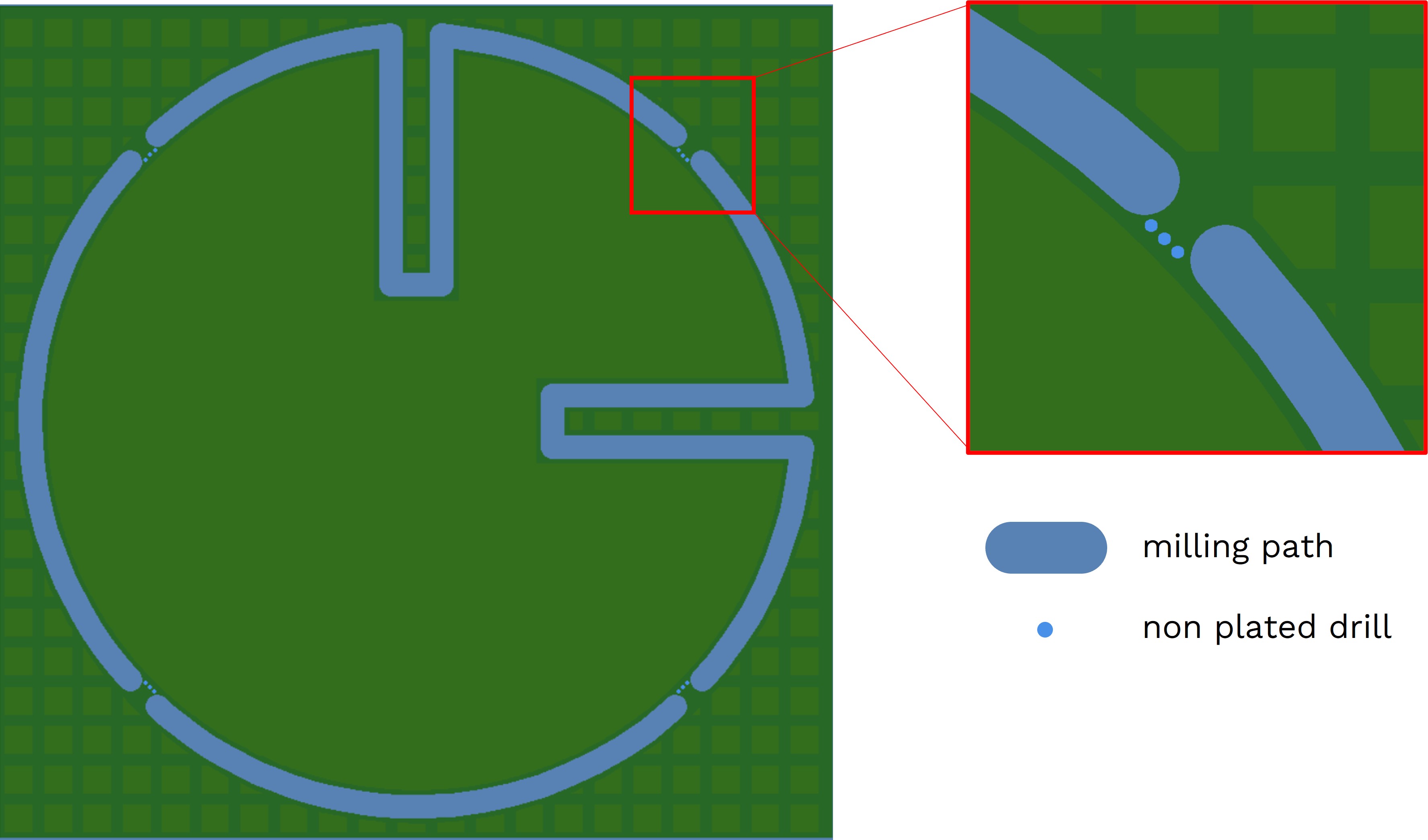
When milling the outer contours of your PCB at the end of the manufacturing process, it is necessary to hold it place. That’s why we define small areas (bridges) around the contour of your PCB, where no material will be removed by the milling tool. Each bridge (except “small pcb”) is provided with at least three separation holes (mouse bites) to ensure an easy release of the board.
Where do we set bridges?
Basically, there are two different groups which determine how and where we set bridges:
Ordinary PCBs : These are PCBs with a simple shape - i.e., with enough straight outer edges (e.g., a rectangle). For those PCBs, the number and location of the bridges is determined during the preparation of the final production data - and thus after the order has been placed.
This means that neither the positions nor the total amount can be displayed in our Board Viewer in advance.
Framed PCBs: This group includes PCBs that we manufacture in a frame:
- Small PCBs
- Non-rectangular PCBs
- PCBs with selected Rapid Registration Add-On
- PCBs for Amazing Assembly
In the listed cases, we use a raster to determine the number and position of the bridges connecting PCB and surrounding frame. The configuration of this raster is based solely on the dimensions of the PCB.
The position and number of bridges can therefore be determined before manufacturing.
Bridge positions of framed PCBs
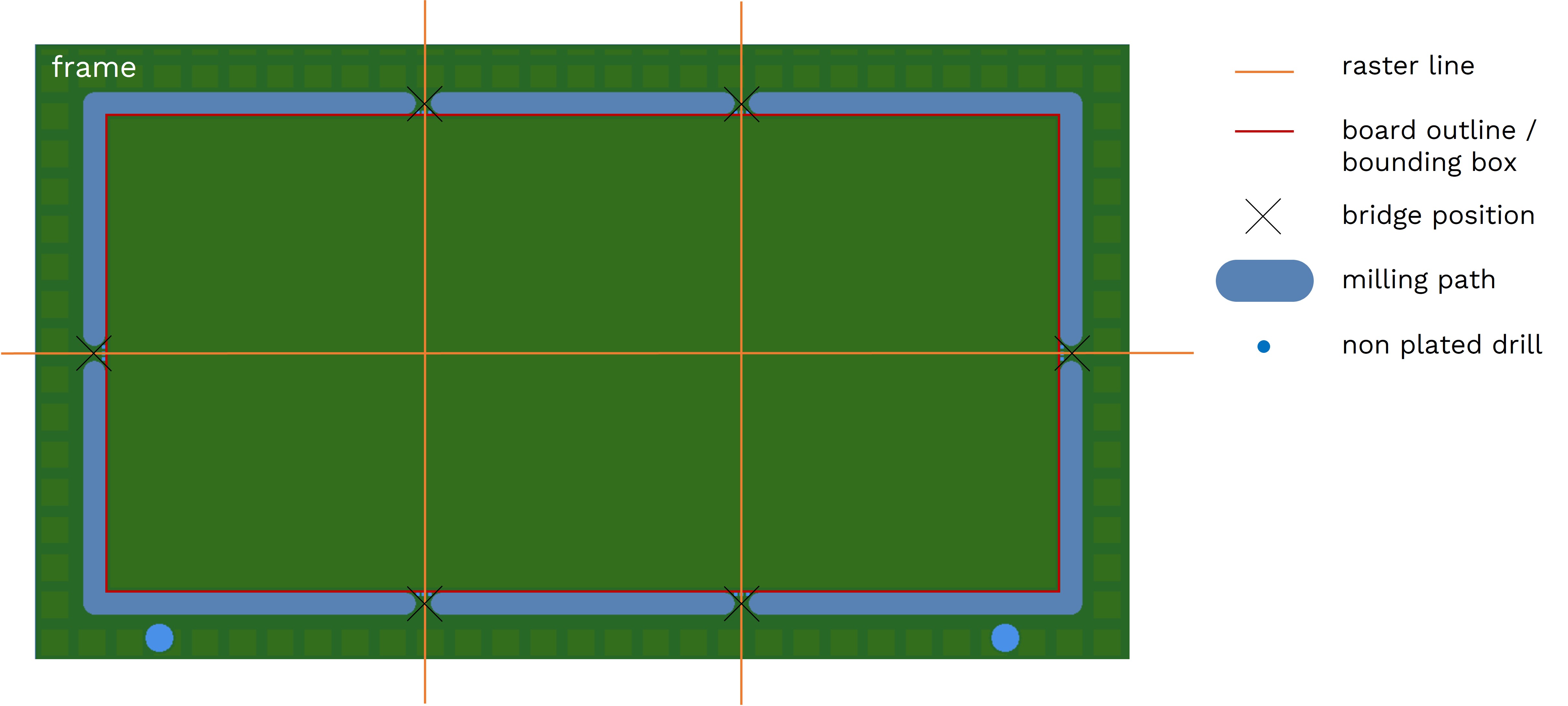
As mentioned before, we use a raster to determine the number and position of the bridges connecting PCB and surrounding frame.
The raster consists of one or more straight raster lines. These straight raster lines run horizontally or vertically. A bridge is placed at each intersection of a raster line with the outer milling path. Since the outer milling path is a closed path, each line creates at least two intersection points and consequently two bridges.
The number of raster lines, as well as their distribution, always follows the same rules:
- height, width ≤ 80 mm: one raster line
- 80 mm < height, width ≤ 160 mm: two raster lines
- 160 mm < height, width ≤ 240 mm: three raster lines, etc.
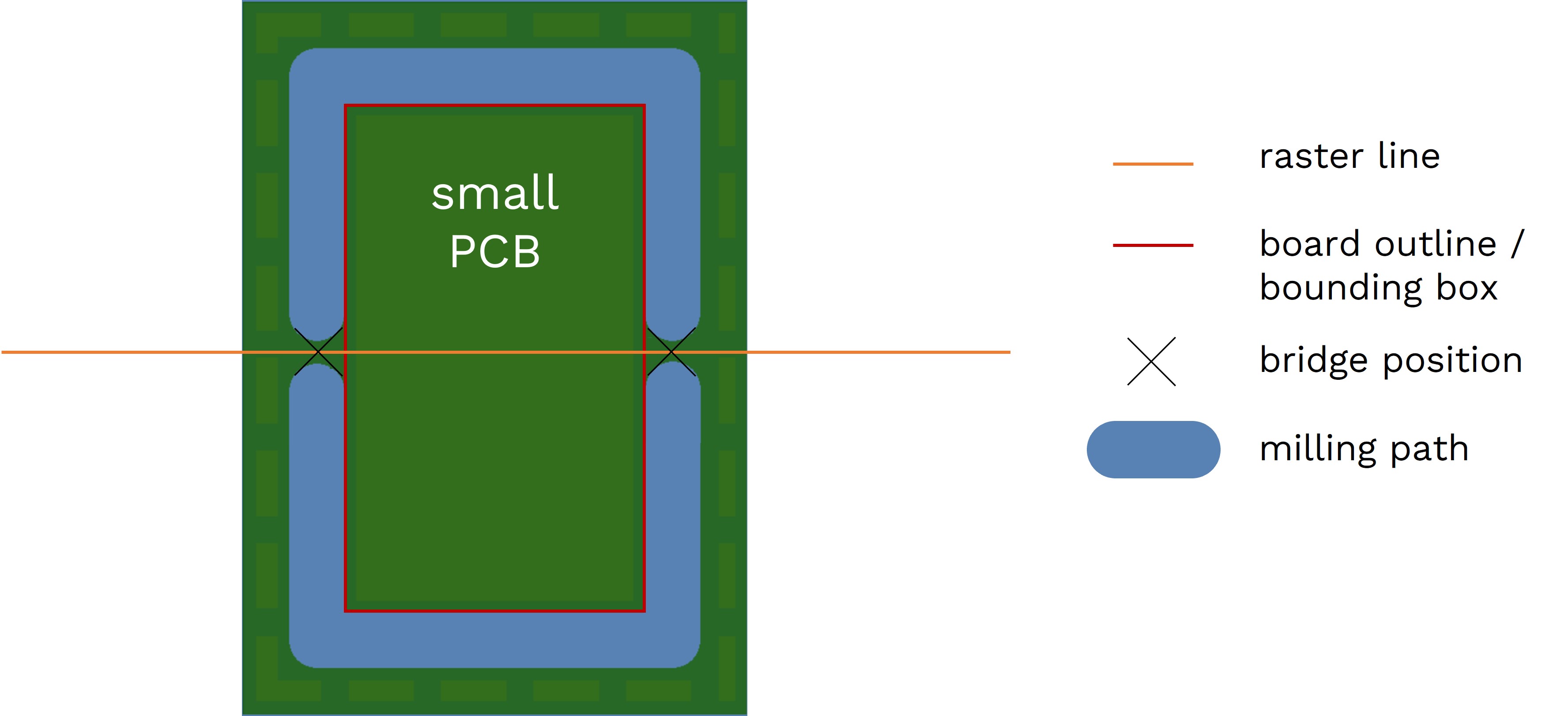
Exception: Small PCB – only one horizontal raster line!
Let’s have a look at an example. Let’s say the oval-shaped (non-rectangular) board below has a width of 120.0 mm and a height of 70.0 mm. According to the rules above, this makes one horizontal and two vertical raster lines. All lines are centered or evenly distributed over the dimensions of the board.
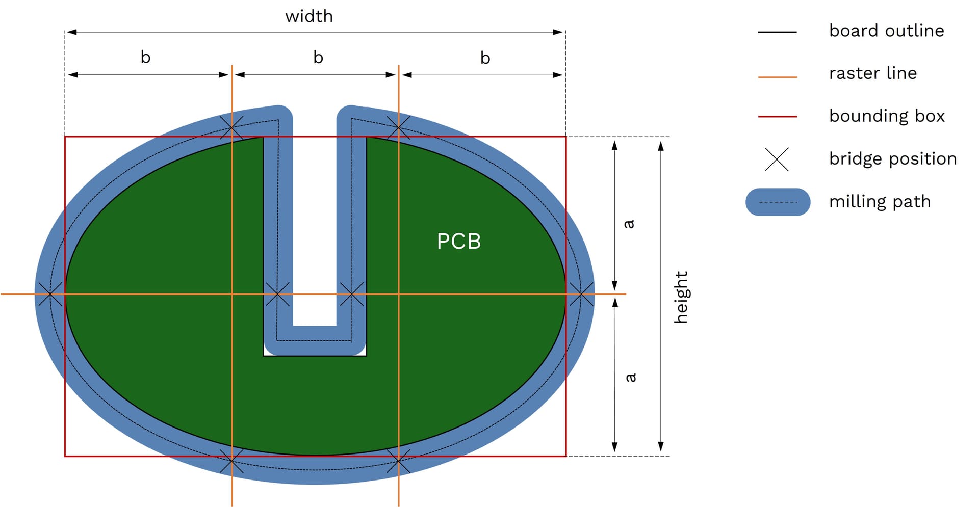
In the sketch you can see that the vertical raster lines each intersect the milling path twice. The horizontal raster line, however, intersects the milling path four times due to the cut-out. That makes a total of eight bridges.
Small PCBs:
Every PCB which fulfills the condition (height + width) < 60 mm (2.36 in) is classified as a Small PCB. Due to their small size, it is sufficient to set a bridge in the middle of the left and right edge to connect it to the surrounding frame.
Non-rectangular PCBs:
If your PCB is not a Small PCB and its shape deviates strongly from a simple rectangular form, we add a frame around it. In this case, we use at least one horizontal and one vertical raster line to determine number and position of bridges. Important: The number of bridges increases with the outer dimensions (bounding box) of the PCB – see raster rule.
PCBs with selected Rapid Registration Add-On
When the Rapid Registration Add-On is the selected, a frame with two 3 mm (0.12 in) mounting holes will be added automatically to your PCB.
PCBs for Amazing Assembly
We manufacture each board that is assembled by us in a subpanel. The position and number of bridges that hold the single board within the subpanel is done in the same way.
User defined Bridges
In most cases, the bridges we place are unproblematic. However, there are cases where the “raster methodology” explained above reaches its limits and leads – in the worst case – to a malfunction of the board.
These include bridge(s), which are placed
- in or close to narrow cutouts
- on segments with Castellated Holes
- on the same position or close to a “large” drill
- under or close to a component, which overlaps the outer contour
- on segments which require a proper finish, e.g., if these segments must be fitted into an enclosure
To take these cases into account, users can provide individual bridge positions in their EDA application. If these meet the necessary criteria, the board will be manufactured in a frame using the bridge positions defined by the user.
How can I define my own bridge positions?
It’s very simple, when you follow the steps below:
Step 1: Determine the required number of bridges:
Think about how many bridges you want to use. Please use the following table as a guide.
Recommended number of bridges = Number of raster lines x 2
Important: At least two bridges are required!
Please note: An insufficient number of bridges can lead to destruction of the board. Misuse of this feature (significantly falling short of the recommended number, very unfavourable placement) can lead to an exclusion of the warranty in case of faulty production!
Step 2: Mark bridge positions in your project using your EDA-application
Each bridge needs to be indicated by drawing a line element. For ODB++ you will have to draw it on a custom layer with the name aisler-bridges, for all other EDA formats you need to draw it on the corresponding board outline layer of your EDA application (e.g., KiCAD – EdgeCuts, Eagle – Dimension (20), …), according to the sketch below:
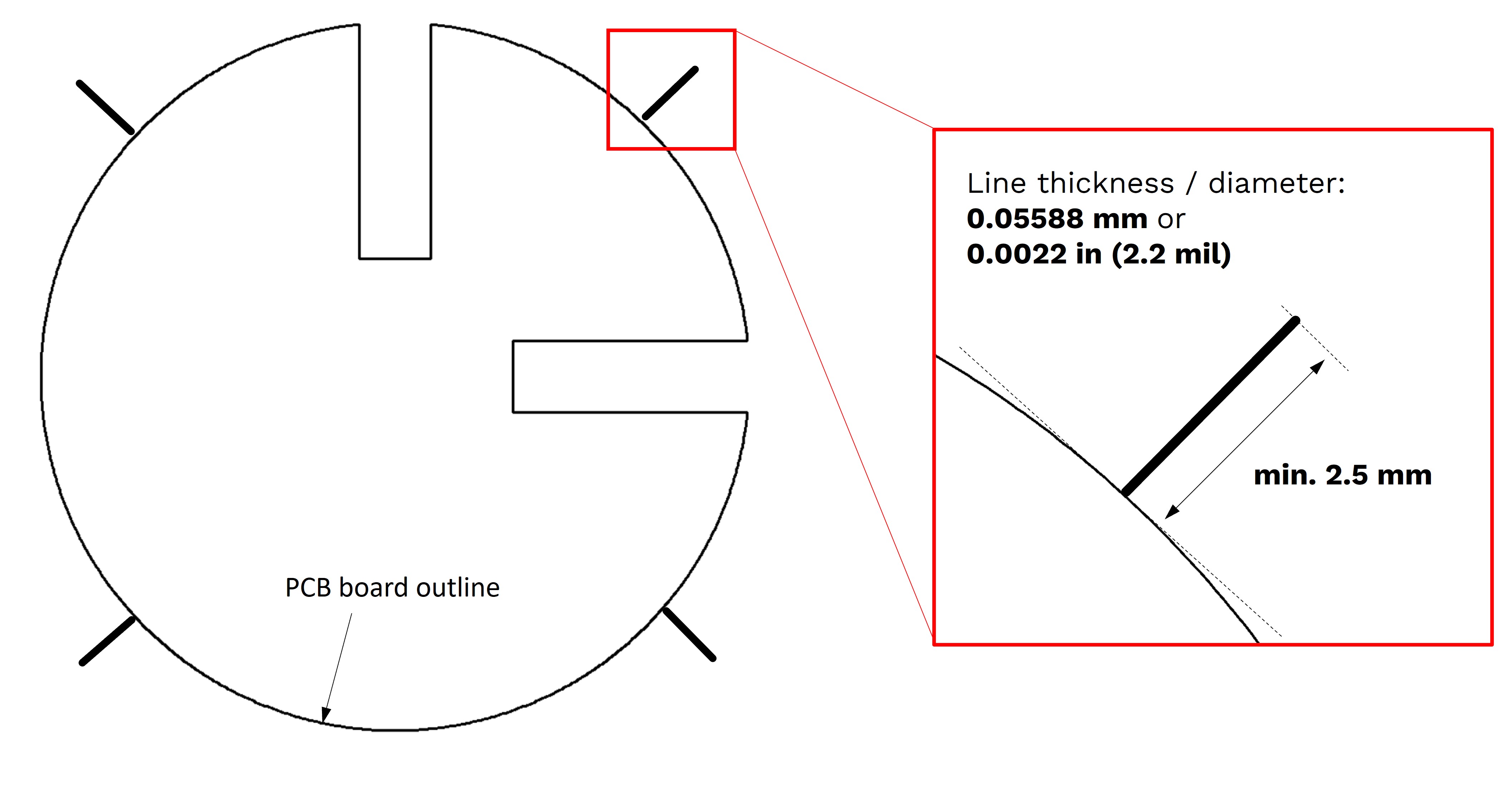
Please take extra care that each bridge marker has a line width of 0.05588 mm / 0.0022 in / 2.2 mil!
Distribute the bridges as evenly as possible! One-sided distribution can lead to loss and damage of the board!
The lines may intersect or touch the board contour, but they do not have to. To avoid influencing the copper filling or error messages when performing the DRC, it is recommended to place the line outside the board contour.
Step 3: Save & upload your project
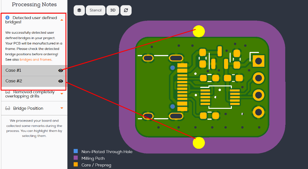
Step 4: Our system checks if the bridge markers are drawn properly (intersection with board outline, respectively the milling path) and if the number of bridges is sufficient. In this case, you will find a Processing Note “Detected user defined bridges.” showing all detected bridges. Currently, bridges will be marked as a simple dot - please check the detected bridge positions before ordering!
Please note: If you can’t find a corresponding Processing Note, we will manufacture your project as usual.
Step 5: Order and receive your PCBs!