Speed Sensor Design Process

Hey, my name ist Leonard and in this post, I want to present my Design Developing Process of a Speed Sensor PCB. I participate in a student racecar construction project and we use Altium for our PCB Design. I like electronics, because you can implement crazy stuff in small spaces and nowadays there are no limits, even for non commercial student projects.
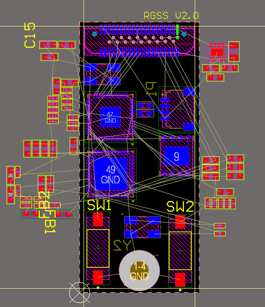
I want to share my Altium Design experience with you. Important to know: The PCB is part of several PCBs placed in one housing. The communication between the PCBs is realized with a Pin Header. Of course, the position of the Pin Header is fixed, so I needed to keep that in mind while arranging all the other components.
The same applies to the Board Outline and a screw hole. Before I started arranging the components, I took a look at which bus systems exist between my IC’s. This helped to place the Components in an efficient way.

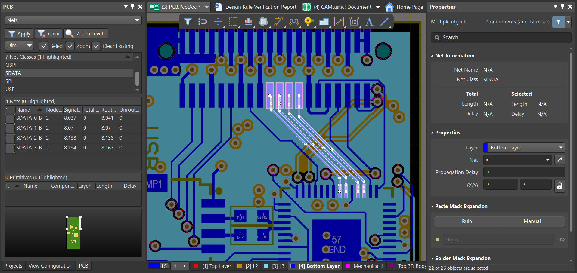
Check out the net class feature Altium provides you with. This gives a good overview about the different netsystems.

The first nets I routed were the differential nets. My design only had one differential net: USB. I rearranged my PCB structure slightly to keep the trace for the differential net as simple and short as possible.

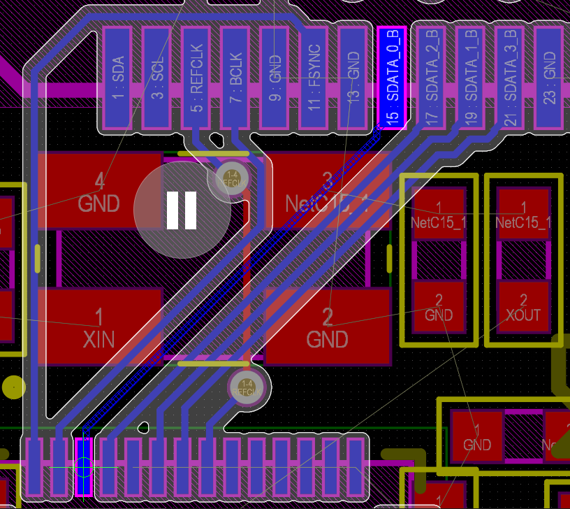
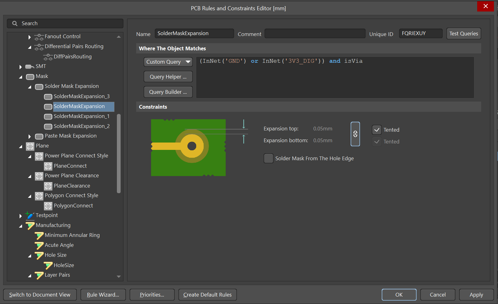
Then I routed the other bus systems. I tried to keep the ways as short as possible and I kept a little distance between the clock trace and the data trace. This should reduce the interference in the bus system. Then I routed all the other smaller components, mostly resistors and capacitors. Most of the capacitors were used to decouple the IC’s, so I placed them directly under the IC’s (on the other side of the board). After that I routed all ground and supply traces. That’s quite easy because my design has four layers. Sometimes, I also use the middle layers for data traces, but normally I use them as power and ground plane. My last step was to arrange the Design Rules according to Aislers fabrication limitations and run a design check. In order to not violate the minimum solder mask width, I had to tend some of my vias. I always tend the vias under components and the Power/Ground Vias. Reason for that: Vias under components cannot be reached after the component is placed, so you cannot use them for measurements on your PCB while debugging. Instead, you risk having some solder bridges under the component and I assure you, that you won’t find them. I have another tip: You can create some special rules in the Design Rule Panel. I created one, to tend all GND and Power Vias, so I didn’t have to tend them one by one.

Last but not least: A colleague checked my design. I highly recommend such a review system, because it helps to spot mistakes before the PCB is fabricated. Also don’t forget to let someone check your schematics before starting the Layout.
Finally, I generated the Fabrication Output Files: Gerber File and NC Drill Files. Don’t forget to hit the “generate separate NC drill files for plated & non plated holes”. Aisler needs this information separately. Afterwards I renamed the Gerber and NC drill files according to Aislers standards. Checkout this Aisler Information Page on how to import the Files to your Aisler Sandbox. Once your design is uploaded, Aisler has a few practical features to check your design. The tool is quite clear and easy to understand. Don’t miss to order stencils, in the case you want to place your components in a solder oven. The order page on the Aisler Website is convenient, because it is integrated in your project overview as well. Now I wait for the PCBs to arrive. Wait for some pictures of the fully assembled PCB!


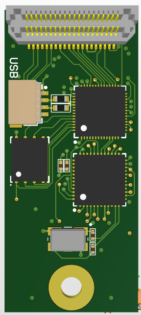
This is only the Altium 3D view :smiley:

What? Do I understand correctly that you tent vias that are under the large QFN center pad? That is a bad thing, at least for the reasons that you stated (that they are out of reach). Can you please share your PCB’s other side, as well as Solder Mask Top and Bottom layer pictures?
You should not have vias under pads tented from bottom, while having them open on top, because after PCB manufacturing, there may still be some residue from etching process, as well as some flux from paste. Those things can boil during reflow, and cause the chip to fly away, or at least move out of position. Also, if there is too much paste, the chip may float, and some side may hang in the air and not solder. If you have vias opened at top and bottom, then residue, flux and excess paste can float into via and out on the bottom side of PCB, avoiding the problems that I mentioned. You should always have them NOT tented on top and bottom. Also, they should be as small as possible, 0.3mm hole for example, so that only small amount of paste flows into them and they don’t steal it too much from pad.
You can only have via tented from bottom if it is also tented from top, or if it is filled with epoxy and plated from top (expensive, used for 0.4mm pitch BGAs).
Look, I know a guy who tents vias under pads from bottom for ages and says that he never has had any problems with that, however, in theory, he should be wrong :smiley: Maybe the manufacturing process has been improved so much that such events happen very rarely, but that is just a good practice.
This does not apply to vias that are outside of components; those can be tented or non-tented if you want to use them as test points.
Also, I would like to point out that decoupling capacitors on the bottom side of the PCB are not always in the shortest path to the chip - the PCB is 1.6mm thick! So putting them on Top layer closer than 1.6mm to chip is actually better. You probably have some trace on top to via, then via to bottom, then trace from via to capacitor - very long, lots of stray inductance. Also, 2-side soldering is expensive, soo it is better to avoid it. I only used it twice - first time 15 years ago when I started studying electronics, in my first PCBs, because I did not know better, and then only now, for a Linux board that has 448 ball BGAs, where yes, decoupling capacitors are only possible on the bottom, under chip. Between now and then, everything always fitted on Top side. Especially if you use 4-layer PCBs - there is so much room on 3 other layers for traces, that components fit on Top very tightly anyway, no need for bottom mounting. Often in 2-layer boards traces take up more space then components! :smiley:
Also, does it only look like it, or do you have only traces on top layer, without copper pour Ground? That is not recommended, because, first of all, PCBs come with 100% copper coverage, and you etch away spaces between traces. Bigger areas without copper mean that you need to etch away more copper, which uses more chemicals, maybe also worse for the environment, but mainly - longer etching time means harder to control thin trace widths, and more risk of too much/too little etching (shorts/opens). Secondly, it is better for EMC, especially for 2-layer boards, because distance between trace and to ground can be down to 0.2 or 0.1mm, but distance to bottom ground s 1.6mm - as thick as the PCB. On 4 layers, Top and 1st internal layers are separated by only around 0.1mm thin prepreg, so they are actually closer than top trace and 0.2mm spaced top ground. But still, better to have them that way.
Also, I don’t see via stitching on your board. I use Altium CircuitStudio, so I put those stitching vias manually, but full Designer has them auto-placed; you can find more info on Google. A 3mm grid is usually fine, up to 1GHz.
Also, do you stop copper pours and traces 0.5mm from PCB edges? I hope so.
Also, you should have Top and Bottom Solder Masks stop 0.3mm from PCB edges. You can easily do that by drawing a 0.6mm thick line on Top Solder Mask and Bottom Solder Mask layers in the same shape as your Board Outline. That way, when your PCBs are cut out using mill or V-Cut, solder mask does not get touched and accidentally cracked, and does not start to peel off (especially in some cheaper manufacturing houses).
Also, it looks to me like your capacitors have a Top Overlay line too close to pads. You should have a 0.2mm space between pad copper edge and Top Overlay line edge. Aisler will probably auto-remove it anyway, but some mass producers don’t; and Top Overlay is not applied very precisely, it can be off by up to 0.2mm (that’s why such distance). I just received such boards from a manufacturer, and if I had put Top Overlay items closer than 0.2mm from pad copper, the paint would be on pads, and some of them would have a bad soldering.
Also, the crystal - you could have placed it closer to the chip; also, you have a long trace from its bottom left pad around the crystal, to capacitor and IC. The trace should have been run under crystal, between right side pads, to have smaller distance between it and the other crystal signal that is on top right pad.
Also, I suggest that you place Designators also on Top Overlay. Then it is easier to find components on the board.
Good luck!
Andris

1 Like

Hey, thanks for your thoughts on my project! The whole tending under components thing was related to components without a GND Pad underneath. There I tend the vias, because you cannot reach them as measuring points and if there are soldered together through to an unlucky mistake in the assembly proccess, you are not able to spot the error. The situation with IC’s having a huge GND pad is different and we also had the discusion about the consequences of having residue from etching proccess inside a tendet via. I only have vias with 0.3mm holes, so we came up with the conclusion that it won’t be a problem. But why taking the risk. I normally do not tend these vias.
I also see the point that my decoupling capacitors are not placed the best way. I hope that this will not cause any problems with the prototyp. I will remember the advise for my next designs.
And yes I have a copper free 0.5mm wide space on the Board Outline. For future projects I will have a solder mask free space as well.
Have a nice weekend
Leonard

Here are some more pictures which I planned to share with you in order to demonstrate my design process:


1 Like