Last Updated: 24/04/2024
Imperial measures are rounded from metric measurements.
Design Rule Files
You want to start right away? We provide design rule files for Eagle, KiCad and DipTrace on Github .
PCB Dimension
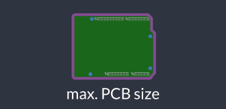
We accept PCBs within these dimensions for our prototype service, contact our support if your design does not meet these criteria.
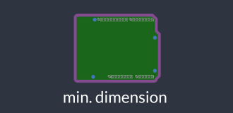
min. dimension
>10 mm / >0.4 in
max. size
400 x 400 mm / 15.74 in x 15.74
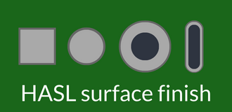
Surface Finish
We use lead-free Hot Air Surface Leveling (HASL) as surface finish for our 2 Layer Simple PCBs, this surface finish is low cost and suitable for many applications.
.
surface finish
HASL
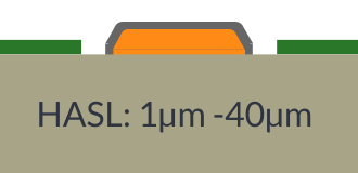
HASL thickness
1 µm - 40µm
Minimum Copper Features
Description
Capability
min. tracewidth
200 µm / 8 mil
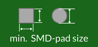
min. SMD pad size
200 µm / 8 mil
Minimum Copper Spacing / Clearance
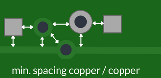
min. spacing copper / copper
150 µm / 6 mil
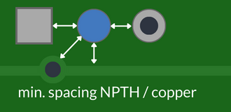
min. spacing NPTH / copper
250 μm / 10 mil
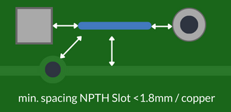
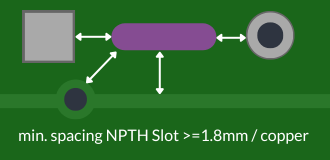
min. spacing NPTH slot <1.8 mm / copper
300 μm / 12 mil
min. spacing NPTH slot >= 1.8 mm / copper
300 μm / 12 mil
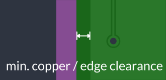
min. copper to edge clearance
300 μm / 12 mil
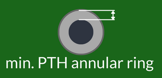
Plated Through Hole (PTH)
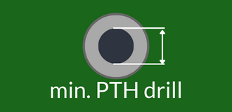
min. PTH drill size
0.5 mm / 0.02 in
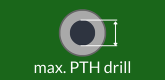
max. PTH drill size
5.6 mm / 0.22 in
300 μm / 12 mil
Vias
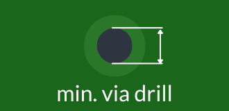
min. via drill
0.3 mm / 12 mil
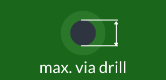
max. via drill
0.5 mm / 20 mil
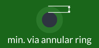
min. via annular ring
175 μm / 7 mil
For economic manufacturing of simpler boards, we may increase the drill size. The annular ring of 175 µm is required to compensate for this.
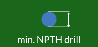
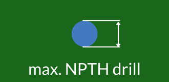
Non Plated Through Hole (NPTH)
0.5 mm / 20mil
5.6 mm / 0.22 in
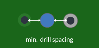
Minimum Drill Spacing
min. drill spacing
300 μm / 12 mil
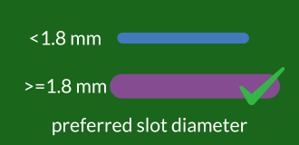
NPTH Slots
preferred NPTH slot diameter
>= 1.8 mm / 0.07 in
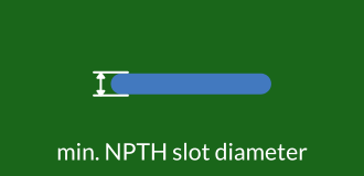
min. NPTH slot diameter
0.8 mm / 0.032 in
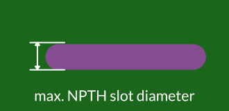
max. NPTH slot diameter
No restriction
PTH Slots
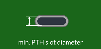
min. PTH slot diameter
0.7 mm / 0.028 in
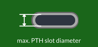
max. PTH slot diameter
2.6 mm / 0.11 in
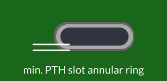
min. PTH slot annular ring
300 µm / 12 mil
Silkscreen
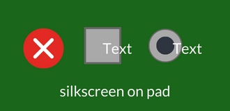
We use Peters SD2692 ink for the silkscreen on our PCBs and apply it using the direct printing method. The smallest supported width is 150 µm / 6 mil, all silkscreen features with a width less of that will be adjusted. Silkscreen printed on pads is not supported, we use openings in the soldermask as reference to cut away / remove the silkscreen in the affected area. Do not use the silkscreen to produce large fillings, designs which cover more than 25% per PCB side will be rejected.
min. silkscreen text height
800µm / 32 mil
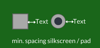
min. spacing silkscreen / pad
125 µm / 5 mil
silkscreen on pad
not supported
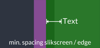
min. spacing silkscreen / edge
400 µm / 16 mil
max. Silkscreen
25% of Board size
Soldermask
We use high-quality Peters Elpemer AS 2467 SM-DG green soldermask which is well suited for the HASL finish. Please refer to our soldermask specification for the electrical properties of the soldermask.
soldermask dam between pads
required for HASL
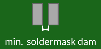
min. soldermask dam
75 µm / 3 mil
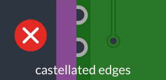
Castellated Edges
Castellated edges are not supported with 2 Layer Simple Boards due to the HASL surface finish, we will automatically select the HD configuration when we detect that a project uses castellated edges.
castellated edges
not supported
Additional Notes
Buried, blind, micro or tented vias are not supported
User-defined subpanels are not allowed, see also here